Test: RAID: 2 x Patriot Warp v3 SSD 256 GB
Solid state disk d. 20. april. 2009, skrevet af The Boss 0 Kommentarer. Vist: 7948 gange.
Billed behandling:
Oversættelse:
Pristjek på http://www.pricerunner.dk
Produkt udlånt af: Shg.dk
DK distributør: MMD
What you don't know about SSD
Since there's a world of difference between a regular HDD and an SSD, we'll begin with uncovering exactly what an SSD is.
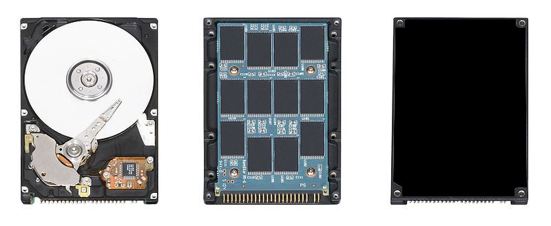
In fact, the only similarities between the regular HDD and the SSD, is that they both store data, use the same interface and have the same standardised sizes.
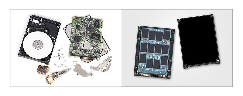
Where the regular HDD uses rotating magnetic platters and a mechanical read/write-head, the SSD has no moving parts at all, and is therefore more rough and less prone to errors. A HDD is actually built from the same principles as the floppy drive with a diskette. This design has been optimised and reinvented quite a few times before the technology has reached its current level. I guess we'll have to agree that this idea isn't exactly new.
So this is where we could be induced into thinking that SSD is built upon an entirely new technology - but it isn't.
An SSD is based on memory chips connected in parallel, and these chips are actually not much different than the RAM that has been a standard component in computers for even longer than the conventional harddrive.
The SSD is still in its very infant stages, so it is quite interesting to follow its developement at the moment, since it is human ingenuity and new ideas, and not the manufacturing-size of chips, that are the most determining factors. So even though the technology has been available for many years, the engineers haven't been allowed to conceive too many new ideas, quite simply since it hasn't been lucrative enough due to the production costs ultimately leading to skyrocketing prices. If the prices are too high, no one is buying, there's no market, and without a market, there can be no money exchange. That's why no one has used time and energy on this technology until today.
Now, its not that the chips being used in SSD's are "ordinary" memory chips like those in a computer. There are two different types of memory chips: Volatile and Non-Volatile. Ordinary RAM chips are volatile, which means that data can only be stored as long as the computer is powered. If the power is cut, all the data disappears and can never be restored. It's very much like if the computer memory formats itself every time the computer is shut off.
The other type - the one being used in SSD's - is non-volatile, which means that the data is stored within the chip, even when it isn't being fed power. There are many different sorts of chips of both volatile and non-volatile RAM, and those used in SSD's are precisely called NAND flash RAM.
NAND refers to the way the data is stored in the chip, and in this world the concerns are about squeezing as much data as possible into as little physical room as possible. The revolutions are happening as manufacturing-size of the chips is made smaller or when a newer and better way of storing the data in the chip is found. We can compare this to the way that music and images are compressed: where wave-files and bitmap-files are compressed into mp3-files and jpeg-files, a data-chip kan be "compressed" in different ways - but with data-chips like in SSD's, there can be no form of compromise, as with mp3's and jpeg's.
All the way down to the cell-level ...
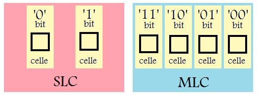
A cell in a NAND flash SSD is either built as 1 bit (SLC) or as 2 bits (MLC). They're physically of equal size, but MLC can contain twice as much data. SLC does, however, have the advantage, that it takes less time to read the contents of the cell, as each cell only contains 1 bit of data where an MLC contains 2 bits. This is due to the way that the contents of a cell is "read", that is done by adding some voltage while waiting for answer, if the cell is empty, the voltage is raised which does that the next cell will be asked and so forth.
An MLC-cell needs to be checked with 4 different voltagelevels, where SLC can make do with just two.
There's not only an MLC- or an SLC-chip located inside an SSD, there's another very important component, the controller. The controller has to manage all the data going back and forth, and a controller handling MLC has up to 3x the work to do compared to one handling SLC. That's why this component is very important, especially in MLC-based disks, where it can have a crucial impact on performance.
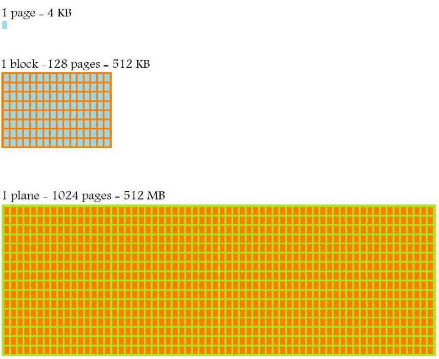
The minimum amount of data that can be handled on an SSD is 4 kilobytes, which is no less than 32.768 bits. This means that the computer works with at least 32.768 bits at a time on an SSD. This may sound like a LOT, but you think otherwise once you get the bigger perspective.
4 kilobytes is also called a "page", and these are once again grouped into blocks. A block contains 128 pages which is 512 kilobytes or 4.194.304 bits.
When you've got 1024 blocks, it is called a "plane", containing 512 megabyte or 4.294.967.296 bits.
512 megabyte is usually the size of the single chips being used in an SSD, but the sights may fool you, as a single chip can actually contain up to 4 layers in one (thats 2048 megabytes (2GB) pr. single-chip).
The performance
NAND flash RAM is common in many devices, ie. USB-keys. The most important factor isn't the speed of one chip, but the amount of chips squeezed together (of course with some performance). The magic is achieved as the chips are joined in parallel, since both size and performance scale upwards with the amount of chips in parallel. In fact, the performance/capacity-relationship can be adjusted "almost as you see fit", and the rule-of-thumb is that you can cut the capacity in half without changing the number of chips, theoretically doubling the performance. When we're scaling like this, it is called data striping, and this is at best comparable to RAID 0.
NAND flash RAM comes in two different flavours: SLC (Single Level Cell) and MLC (Multi Level Cell). The difference is that SLC is capable of handling each bit individually, whereas MLC can read and write bits individually while only being able to "reset" (delete) bits in blocks (gates) at a time (see the picture above). This makes SLC a bit faster than MLC, but MLC is still cheaper to manufacture.
With this knowledge we'll move on the next page where we're going to take a look at the specifications.
Anmeld
Information


